

Check out what we did as a group here!
Okay, so for the group assignment, we were supposed to:
I chipped in by using these tools:
We needed to get some real data, so I used the multimeter to check voltage and the oscilloscope to look at some DC signals. I used the Adafruit Feather Sense nRF52480 to create the signals and voltage. Here's the code I used to generate a signal:
void setup() {
  pinMode(13, OUTPUT);
  pinMode(12, OUTPUT);
}

void loop() {
  digitalWrite(12, HIGH);
  digitalWrite(13, HIGH);
  delayMicroseconds(100); // About 10% duty cycle @ 1KHz
  digitalWrite(13, LOW);
  delayMicroseconds(1000 - 100);
}
To measure the voltage, I used the Terminator TMM7201 multimeter. I set it to measure up to 20V. The Adafruit Feather Sense nRF52480's datasheet *probably* says 3.3V, because that's what it's *supposed* to be. Easy to remember!
But, the *actual* voltage can vary a little because of manufacturing, temperature, and what's connected to it. And multimeters aren't perfect either.
So, seeing 3.27V instead of 3.3V? No big deal!
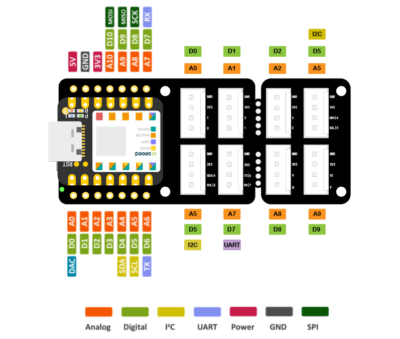
For this assignment, I designed a custom PCB using KiCad based on the Grove Shield for Seeeduino XIAO. I used parts from the Fab Lab inventory and added my own touch. This board is meant to help interact with I/O devices easily using the XIAO ESP32C3. I’ll walk you through how I used KiCad, from adding components to routing the board, and how I fixed the problems I ran into.
For this week's assignment, I decided to design a custom shield that makes it super easy to connect input and output devices without worrying about wiring things the wrong way. One of the common issues I’ve faced when working with sensors or actuators is accidentally flipping VCC and GND — and well… that usually ends badly.
To avoid this, I took inspiration from the Grove Shield for Seeeduino XIAO, which has a nice clean layout and uses Grove connectors to keep things organized. I really liked how simple and intuitive it is to use Grove cables — no guesswork, just plug and play.
My custom board will mainly be used in my final project, where I’ll have multiple inputs and outputs to deal with. So having a reliable and easy-to-use expansion board that connects cleanly to the XIAO ESP32C3 makes my life a lot easier.
Reference design for Grove Shield that inspired my custom board.
I’m using KiCad 9.0 to design everything — from the schematic to the final PCB. It’s a powerful tool once you get the hang of it, and the cool thing is that everything is in one place: schematic, PCB layout, footprint editor, all of it.
The first thing I did was create a new project. Pretty straightforward — just go to File > New Project, give it a name, and KiCad sets up all the files you need automatically.
After that, I jumped into the schematic editor. Before adding any parts, I made sure to check the grid and setup. I usually use a 0.1 inch grid for the schematic and adjust it later if I need more precision. It's also important to set the design rules early on, especially for the PCB — I’ll show screenshots of that in the next part.

Setting up the schematic grid before placing components.
To add components, I used the Symbol Editor. I searched for the parts I needed and dropped them into the schematic. For footprints, I used the Footprint Editor and matched everything with either the built-in library or custom ones.
Global Labels like VCC, GND, SDA, and SCL helped keep the schematic clean and easy to follow.
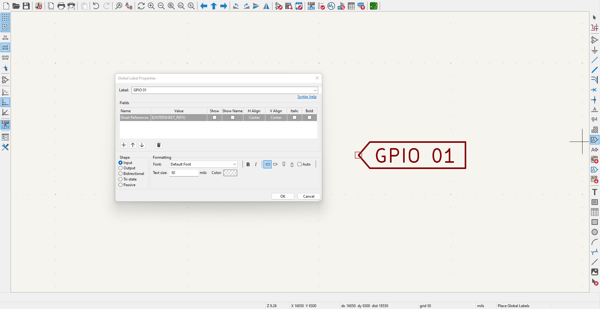
Using global labels instead of long wires keeps the schematic clean.
I downloaded the Fabcloud component libraries from GitLab and added them to KiCad via Preferences > Manage Symbol Libraries and Footprint Libraries.
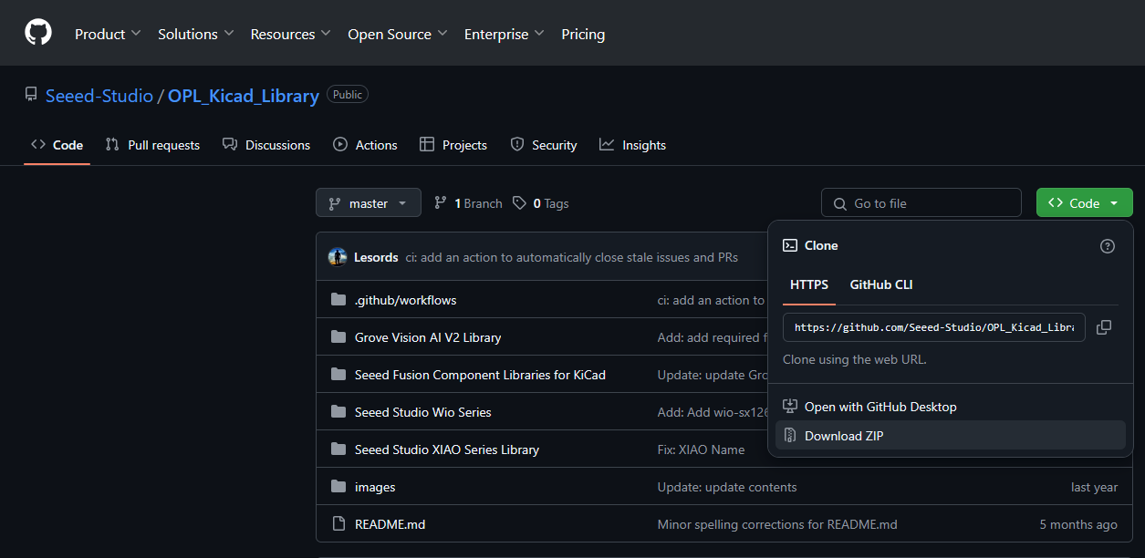
Adding the Fabcloud component libraries into KiCad from GitLab.
I added the XIAO ESP32C3, Grove connectors, and passive components, and wired them using Net Labels. A minor hiccup was updating the XIAO symbol manually to fix missing pin names.
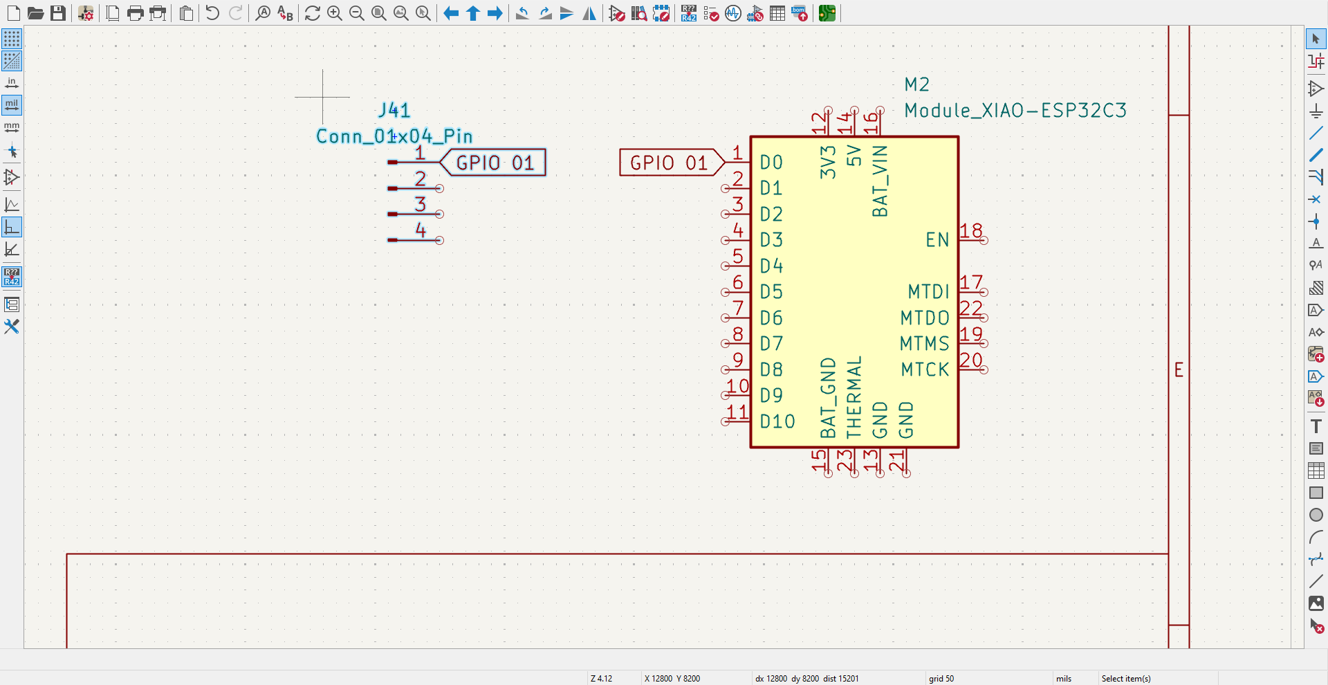
Wiring components with Net Labels makes the schematic cleaner and easier to follow.
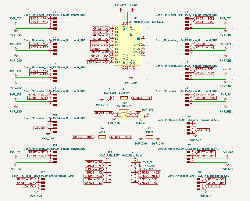
Complete schematic of my Grove-style expansion board.
I used CvPcb to assign correct footprints. Using the footprint filter helped match each symbol properly. One issue was that the 4-pin Grove connector only had through-hole footprints.
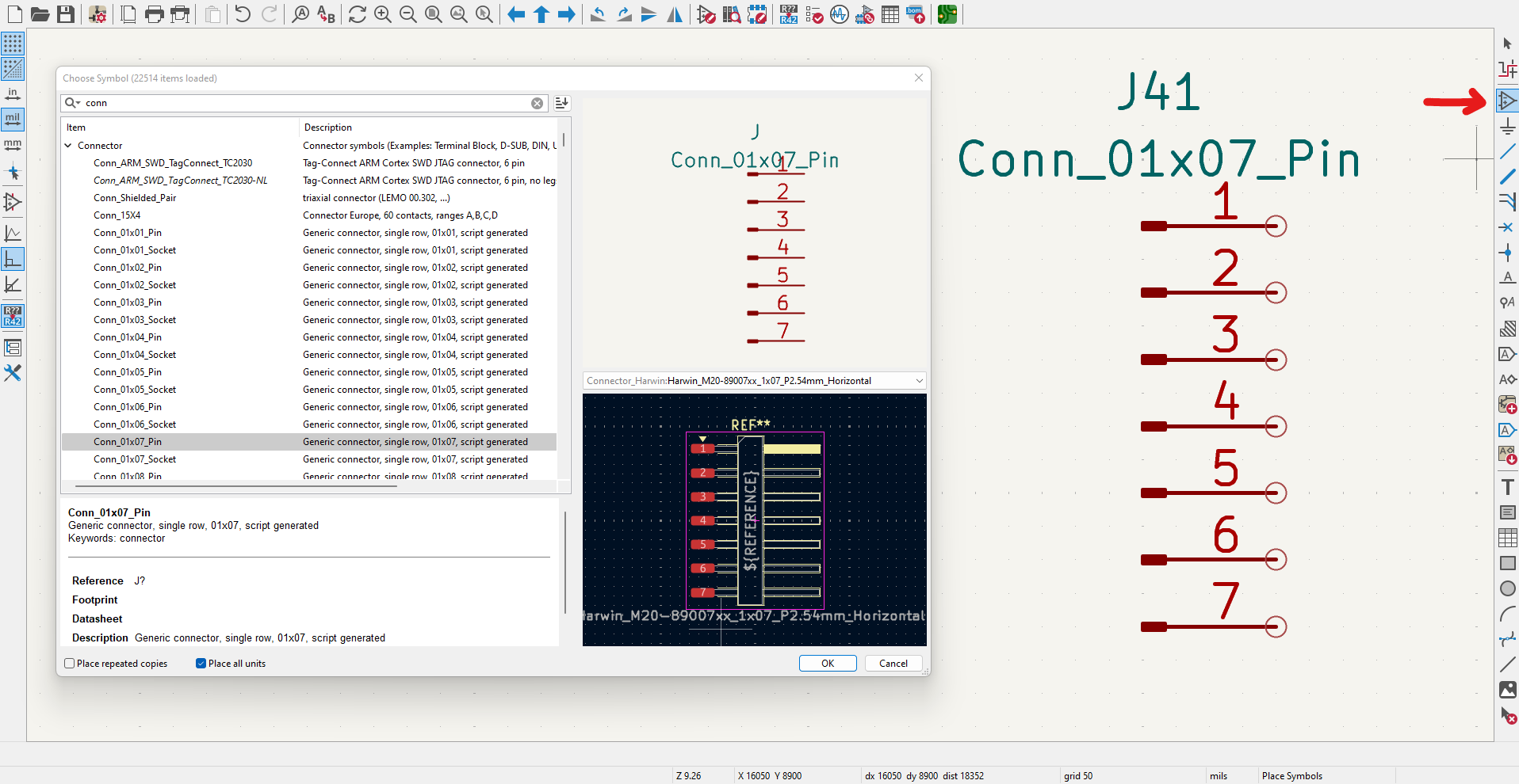
Assigning correct footprints to my schematic symbols using CvPcb.
I found a footprint repo on Seeed Studio’s GitHub and edited the through-hole footprint to make a custom SMD version using the Footprint Editor.
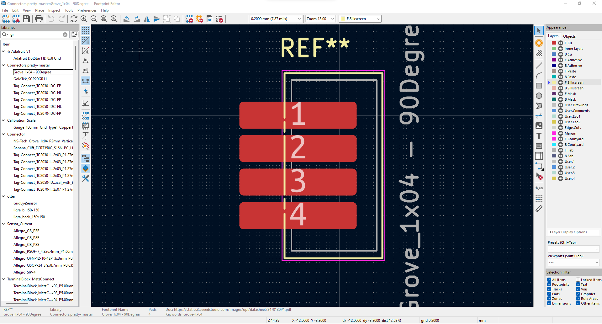
Custom SMD footprint I created for the 4-pin Grove connector.
I arranged my components with the XIAO in the center and Grove ports around it for clarity. I set my trace width to 0.8mm to keep things reliable and easy to route.
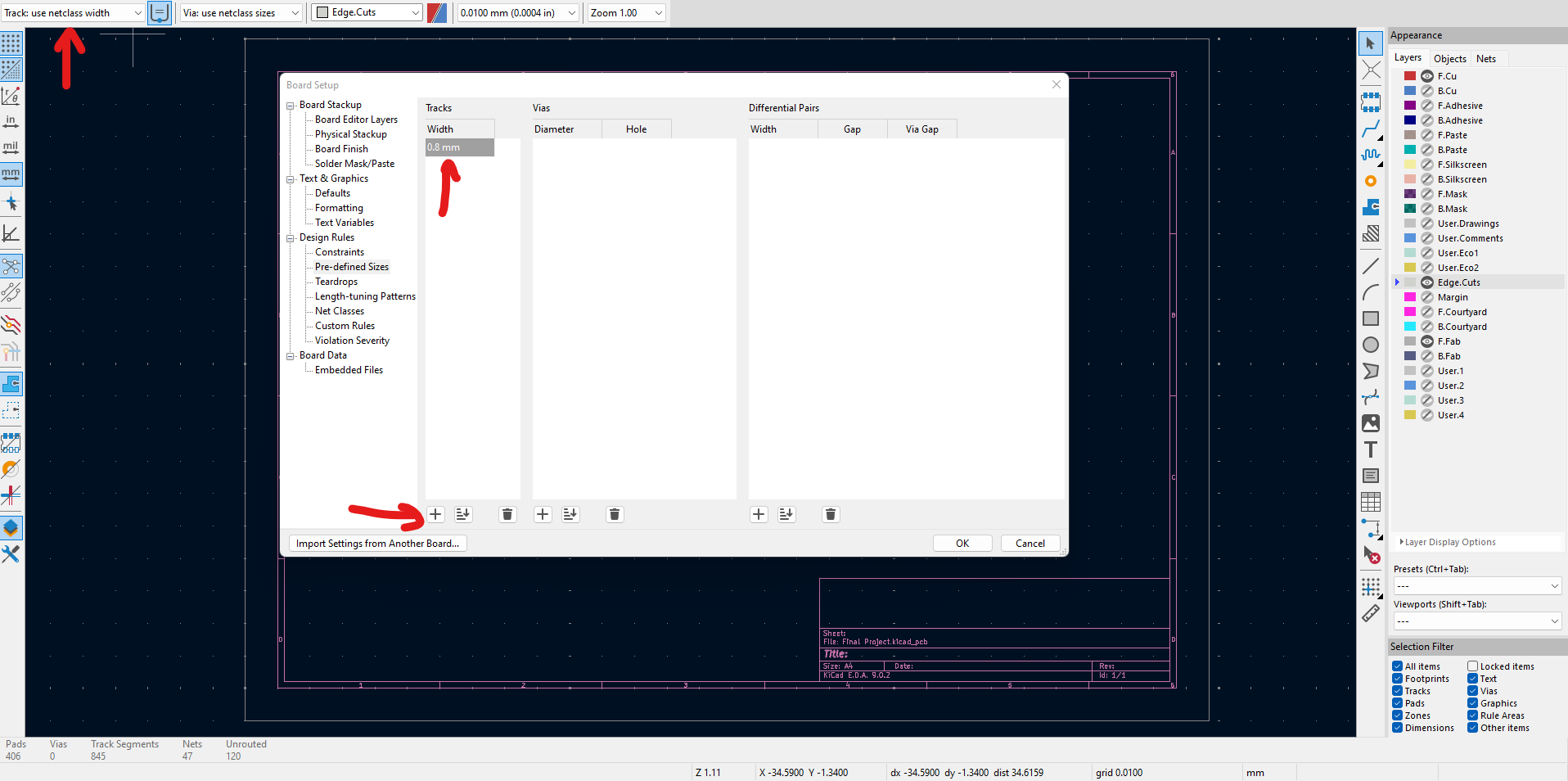
Setting up 0.8mm trace width in the KiCad design rules editor.
All routing was done manually with 45-degree turns — no 90° angles to avoid signal issues and fabrication troubles.

Final routed PCB layout with all connections completed.
One challenge during routing was tight trace paths, which I solved by using 0-ohm resistors as jumpers. It worked great and helped me stay on a single layer.
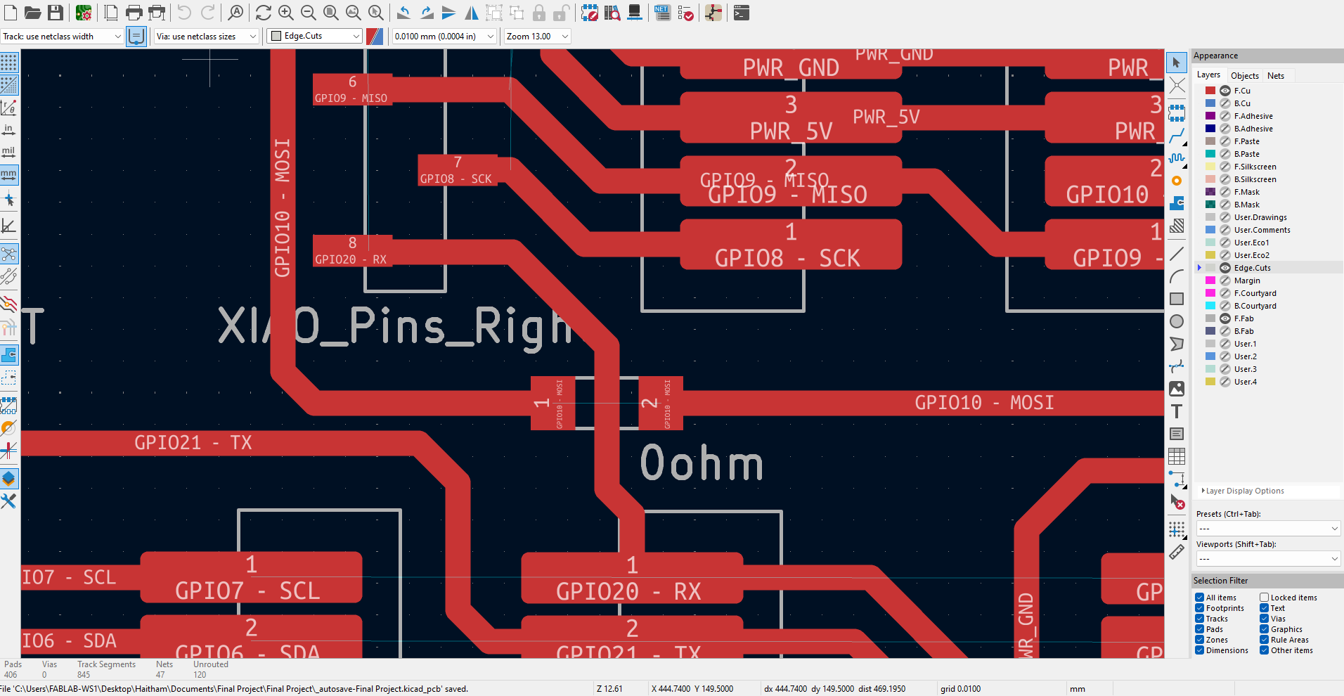
Used a 0-ohm resistor as a jumper to complete a tight routing path.
To export Gerber files: File → Plot → select F.Cu, Edge.Cuts, Silkscreen, and check Protel format. Then click "Generate Drill Files" and enable Excellon format.
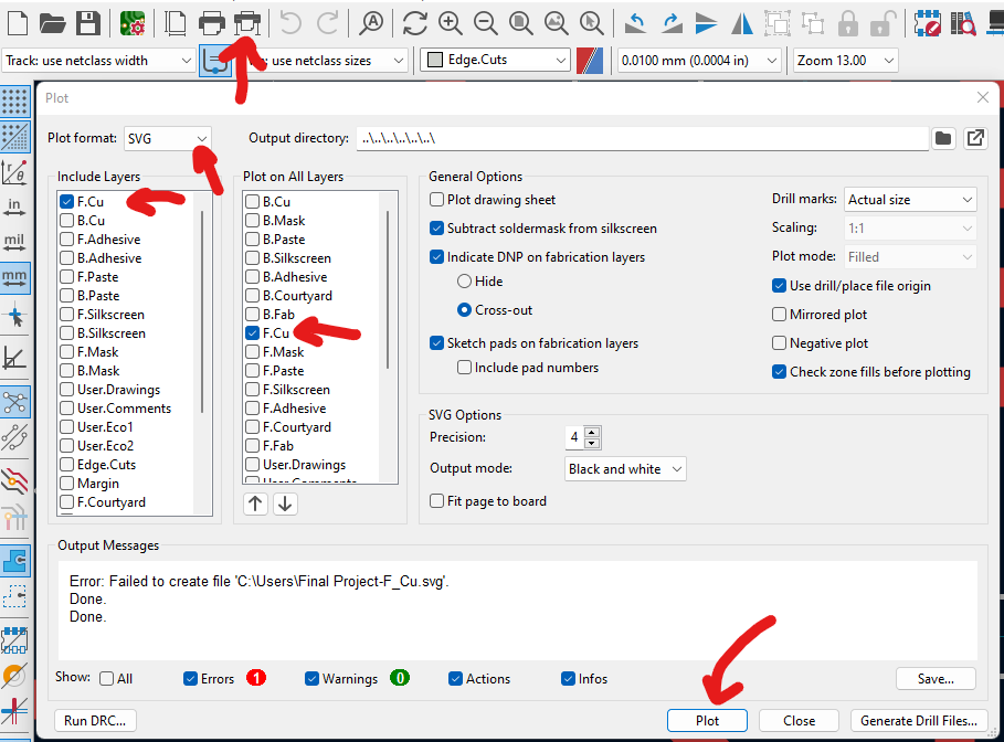
Gerber and drill files generated using KiCad’s Plot and Drill tools.
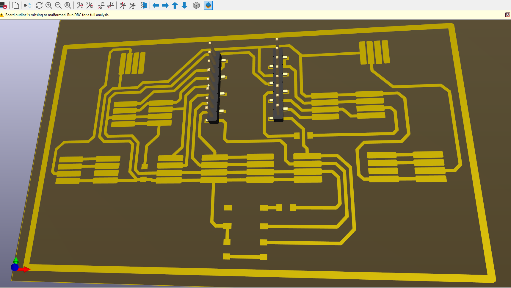
I uploaded the zipped Gerber folder to PCBWay and previewed the board in 3D before submitting.
This project helped me understand real-world component matching, manual routing, and footprint editing. I picked up new KiCad shortcuts (like L for labels and G to move with wires) and learned the value of planning layout first.
Hero shot of my custom Grove-style shield for XIAO.
Included Files:
This board follows Fab Academy inventory guidelines and is ready for anyone to build or improve.