Electronics Production
Overview
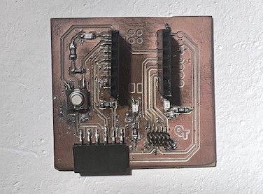
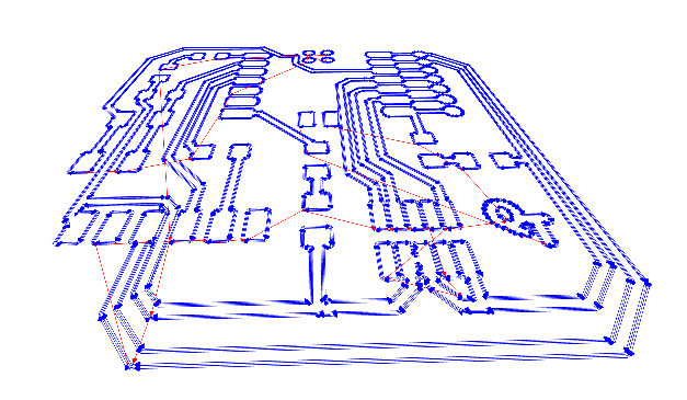
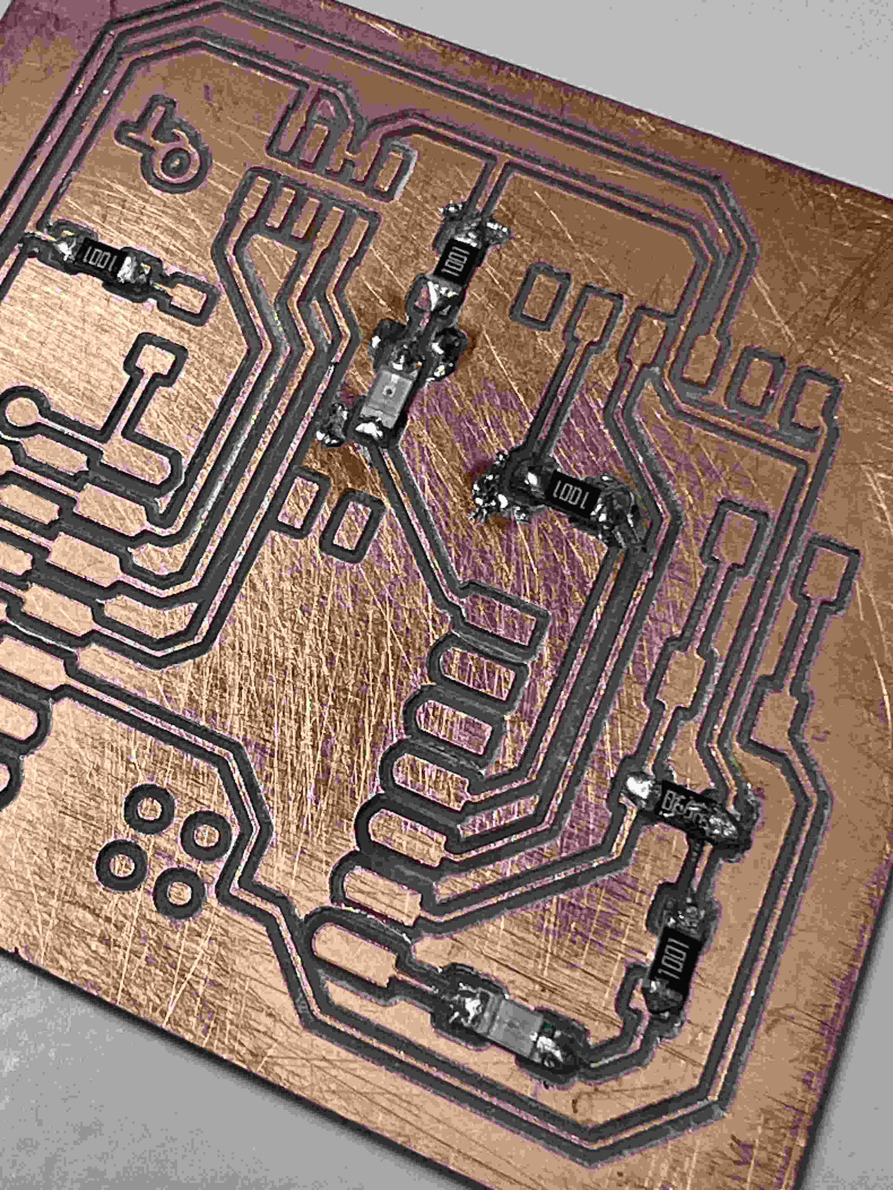
This week is my first time ever producing electronics, or a PCB. In this assignment, I tested the milling machine and found the design rules for in-house PCB production, you can find details about the test [here]. Then I used the findings to produce a PCB, which is the Quentorres created by Quentin Bolsée and redesigned by Adrián Torres.
This TikTok is a recap of the whole process of me producing the PCB. Details, files and all screenshots are found in this page. [The language of the video is Arabic but you can turn on auto translation.]
@santhewitch #pcb #electronics #bahrain ♬ original sound - null.
What is a PCB?
PCB stands for Printed Circuit Board. It is a way to connect electronic components together with conductive material for them to function. There are different types of PCBs, and different ways to produce them. A PCB can be single-sided PCB, double-sided PCB, or multi-layered PCB. Added to this, electronics components assembled in the PCB can be of different types, through-hole or surface-mount.
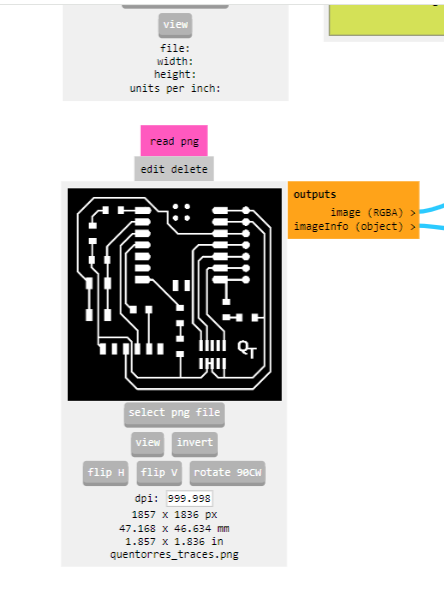
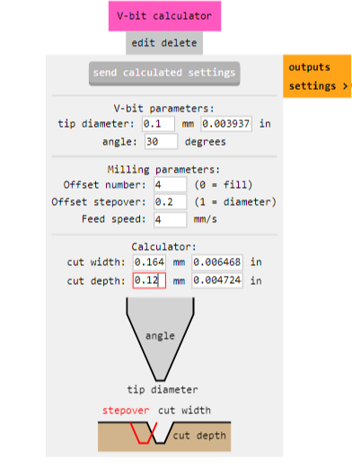
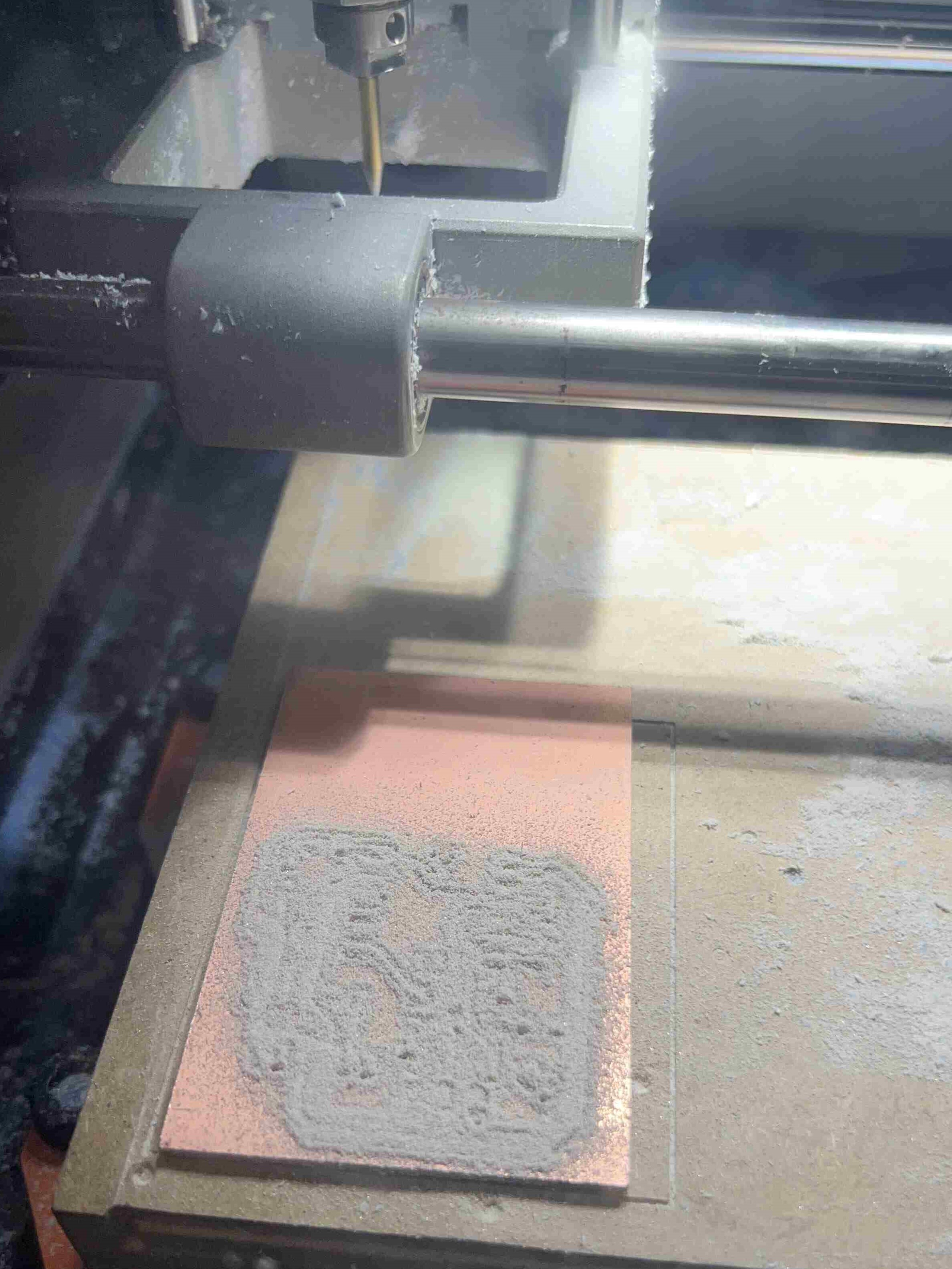
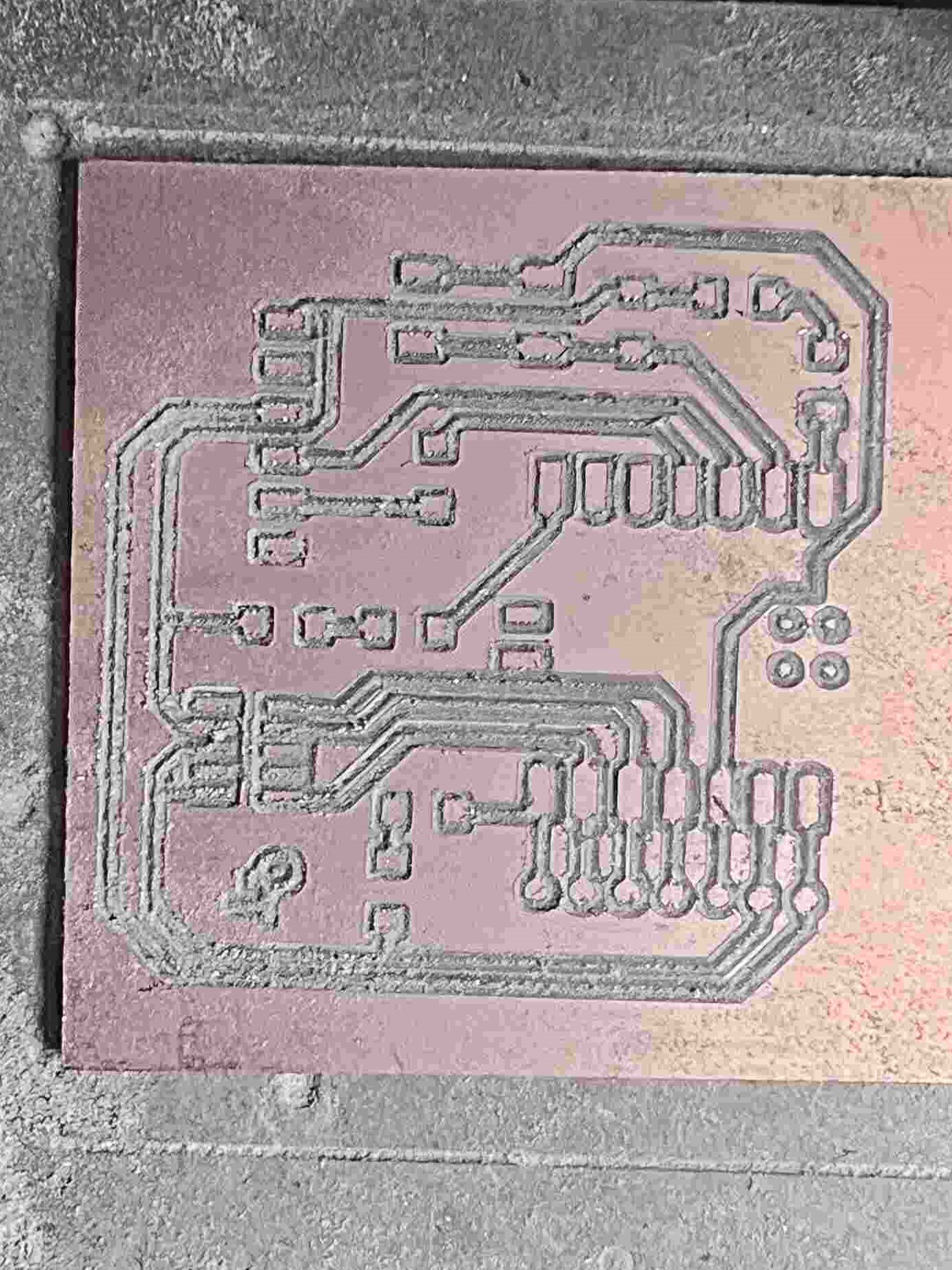
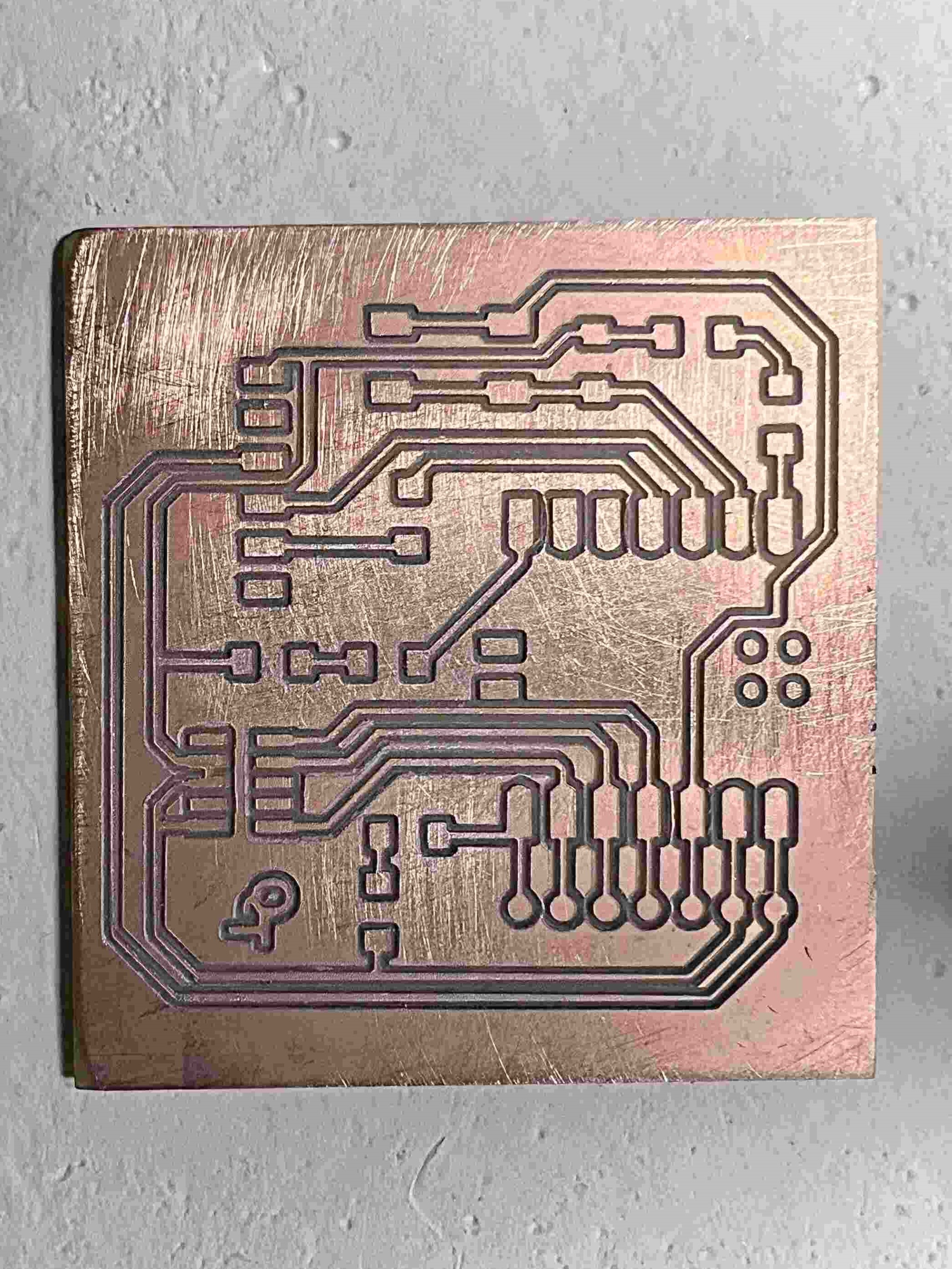
Prepare your Traces
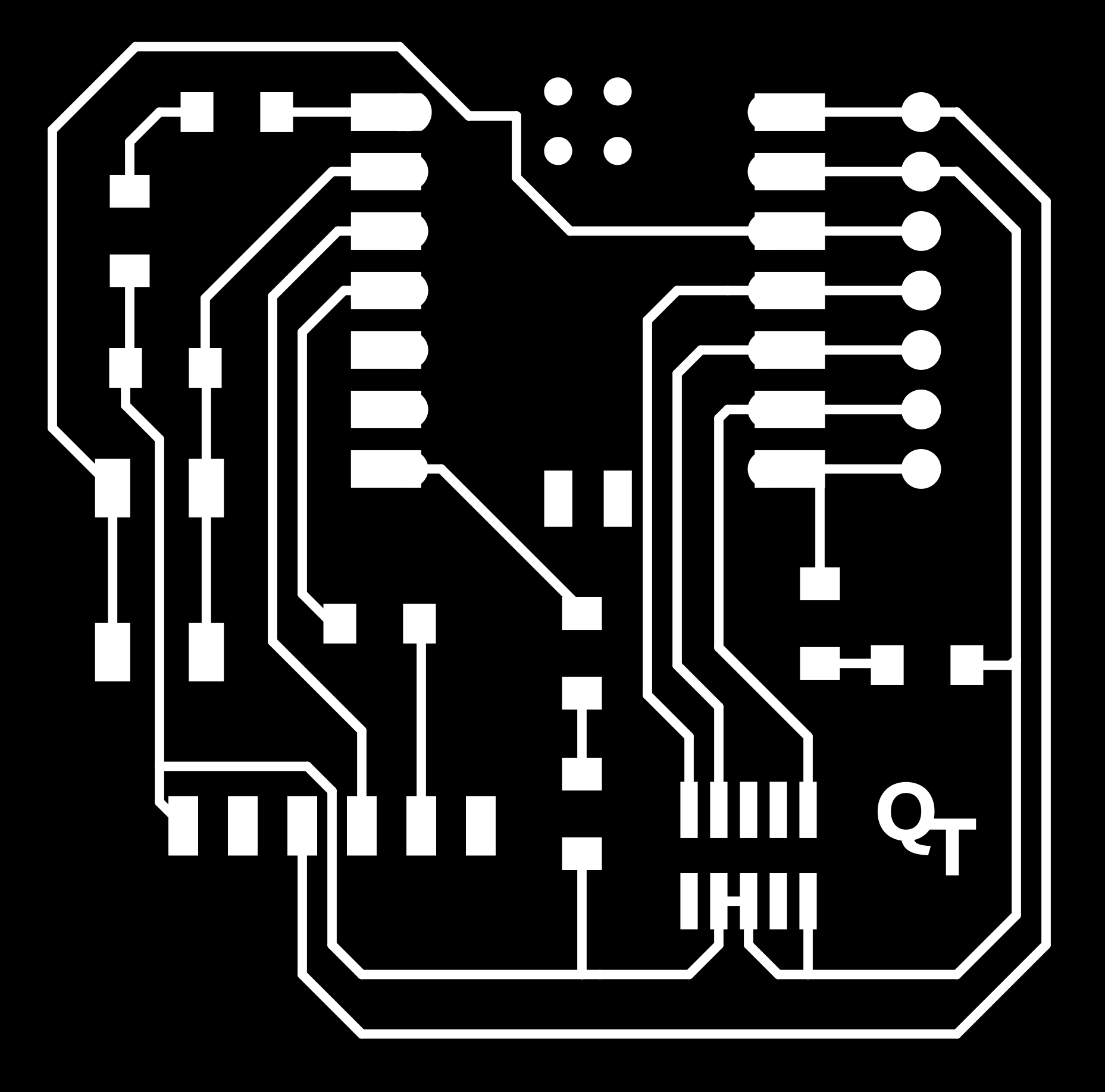
We are producing Quentorres Development Board, the design, schematics, and all of the steps to produce it are all documented here


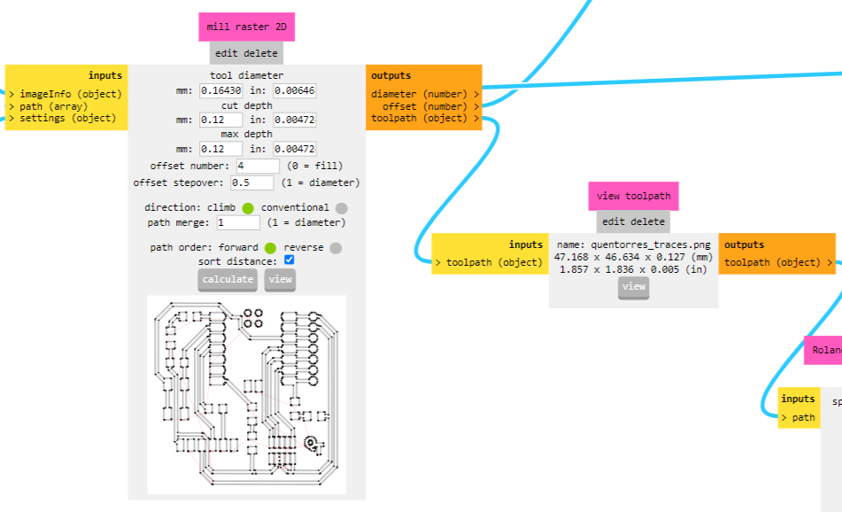
MODS Project CE
- angle: 30
- cut width: 0.164 mm
- cut depth: 0.12 mm
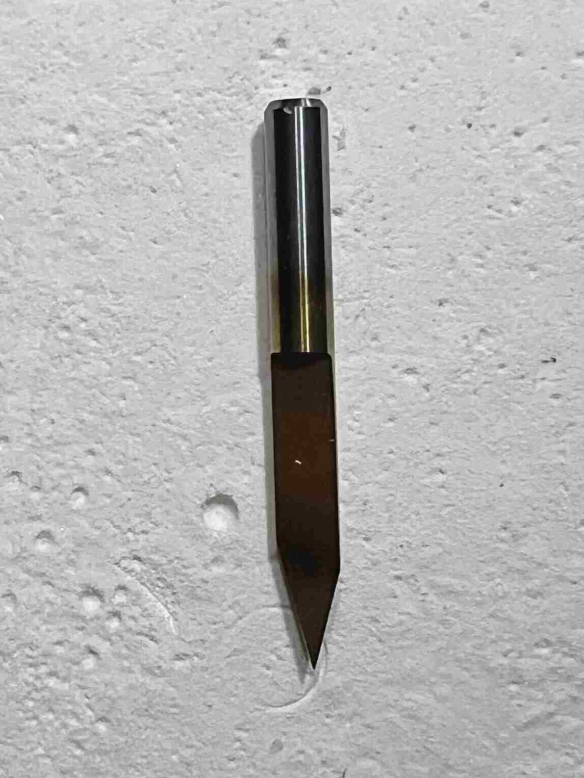
Change the following according to the bit:
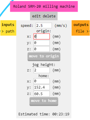
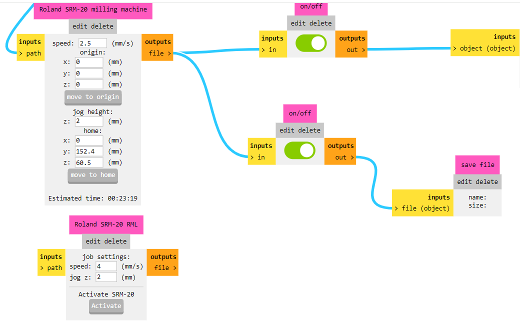
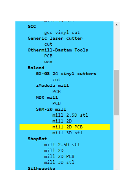
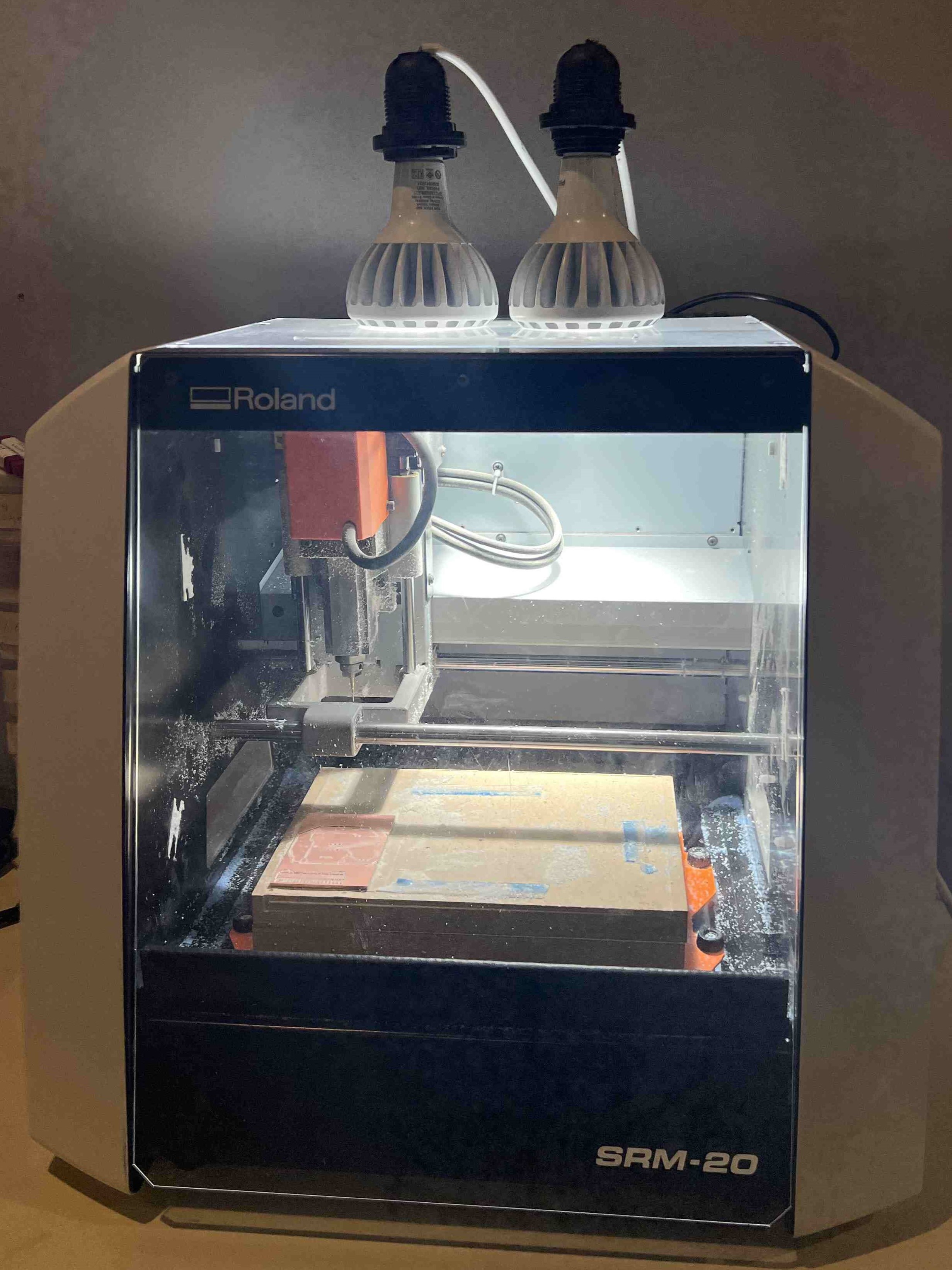
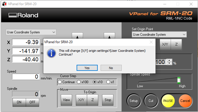
Setup your Machine
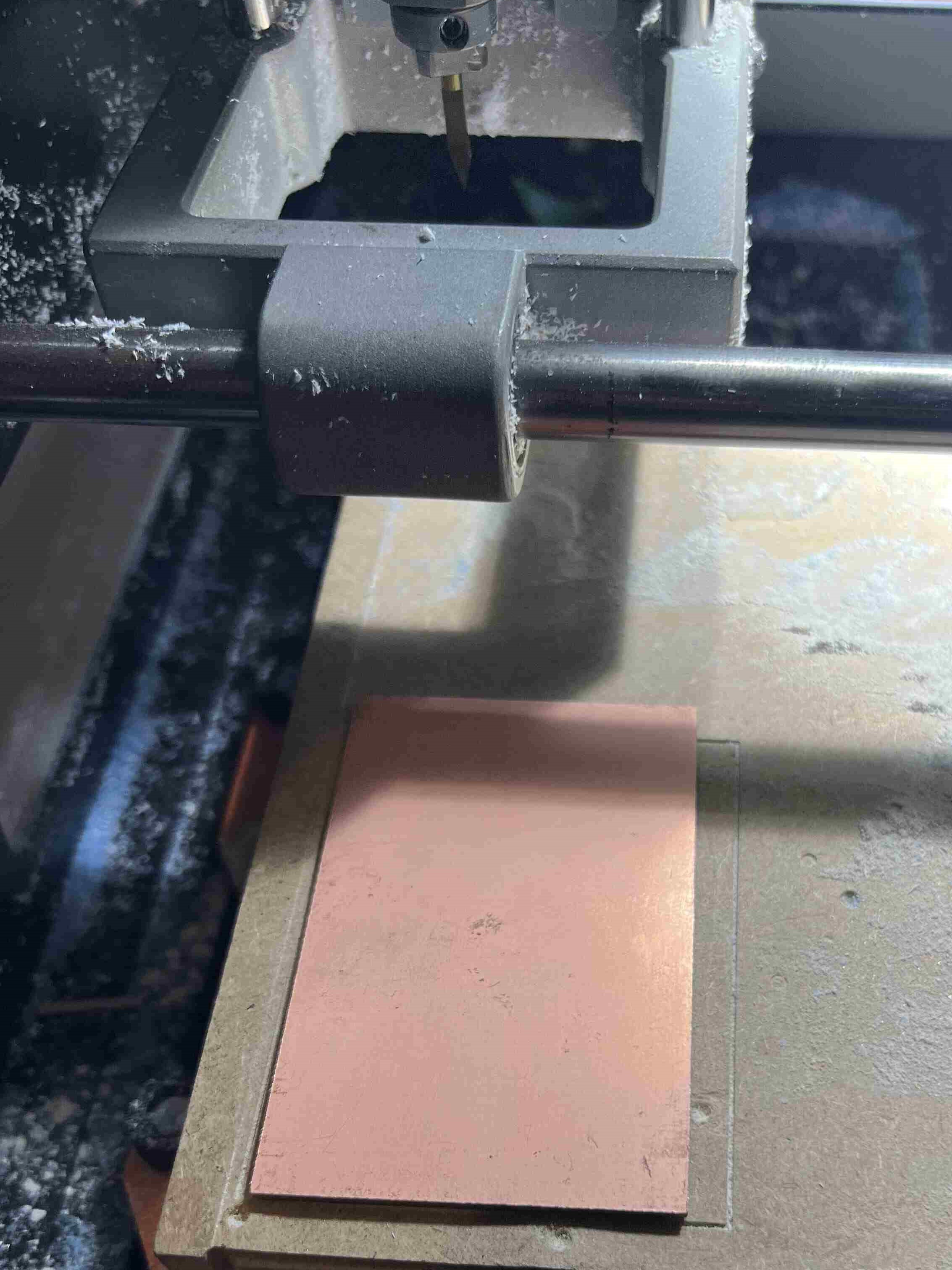
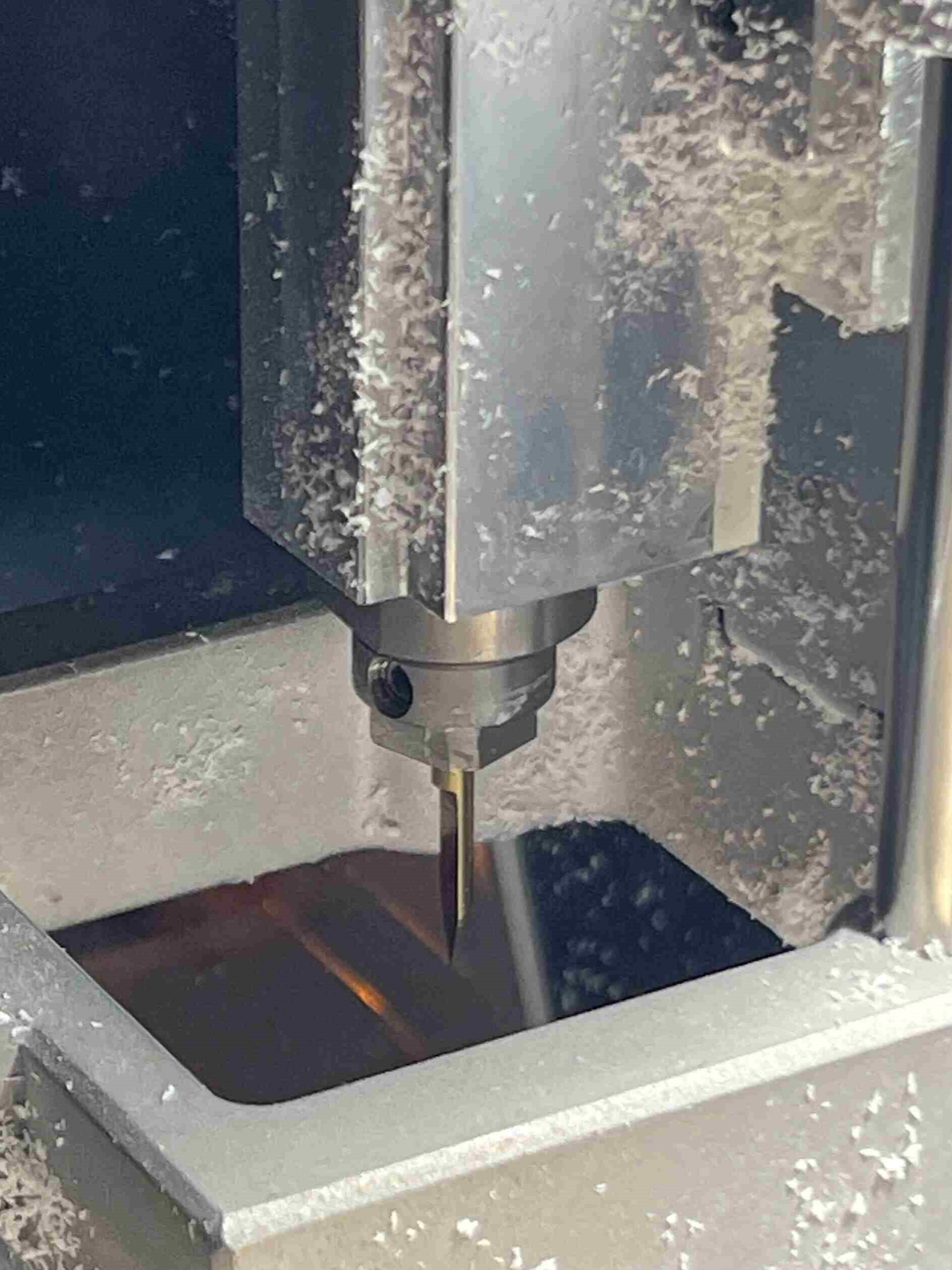
VPanel for SRM-20
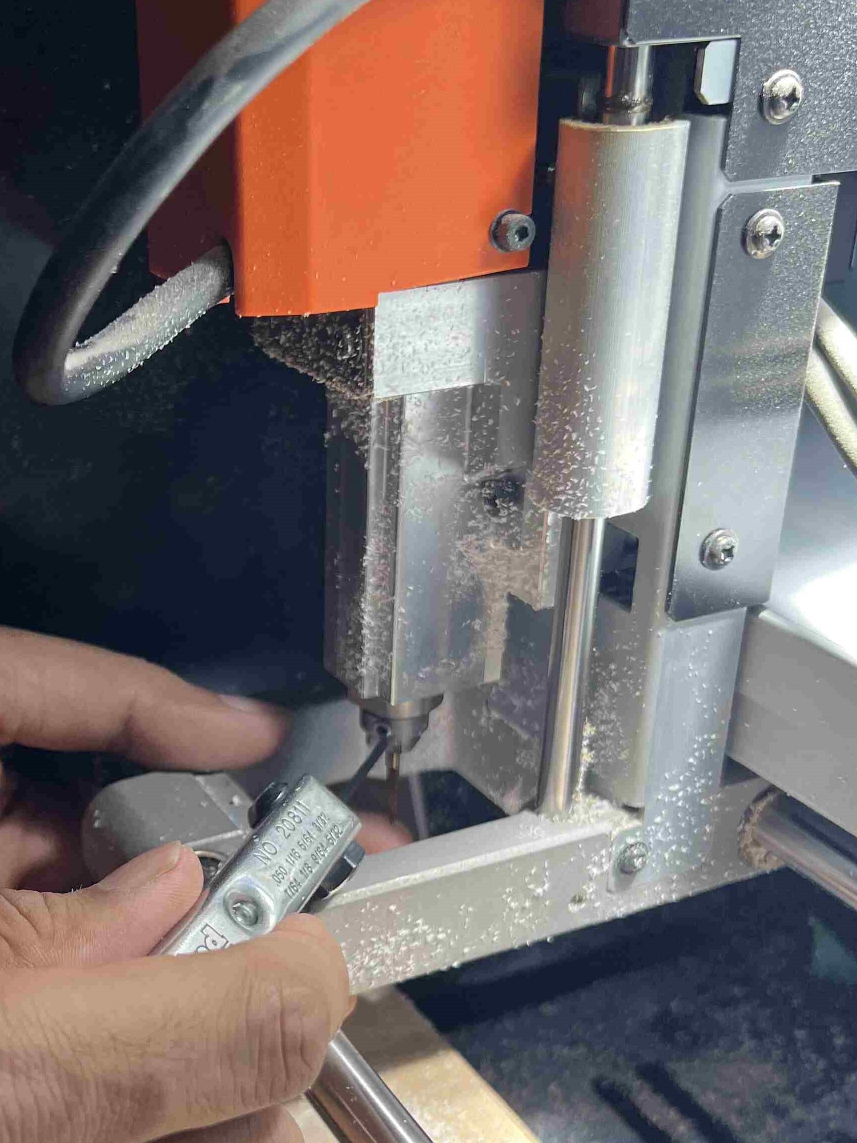
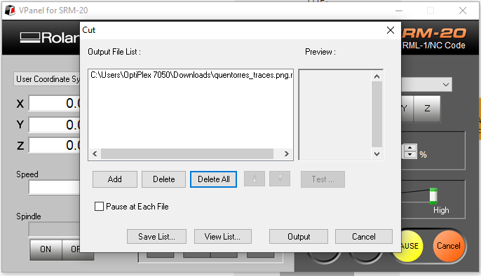
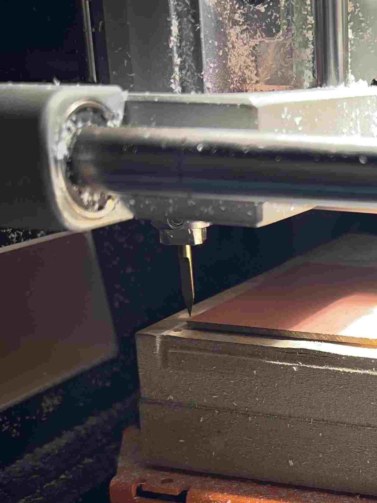
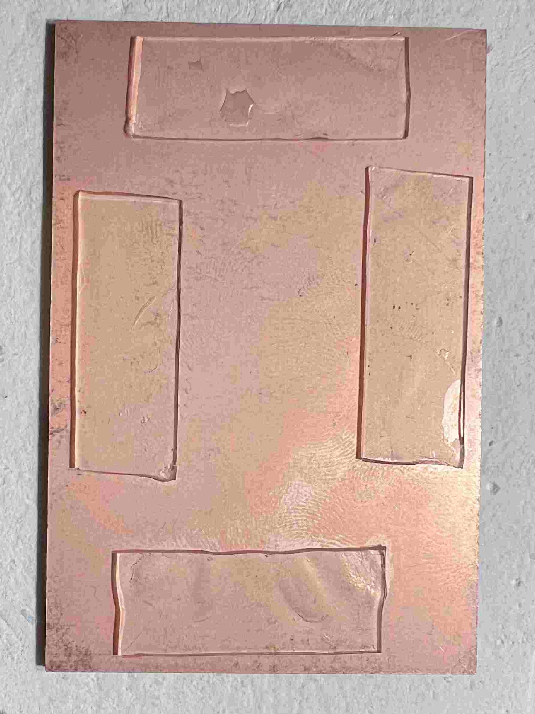
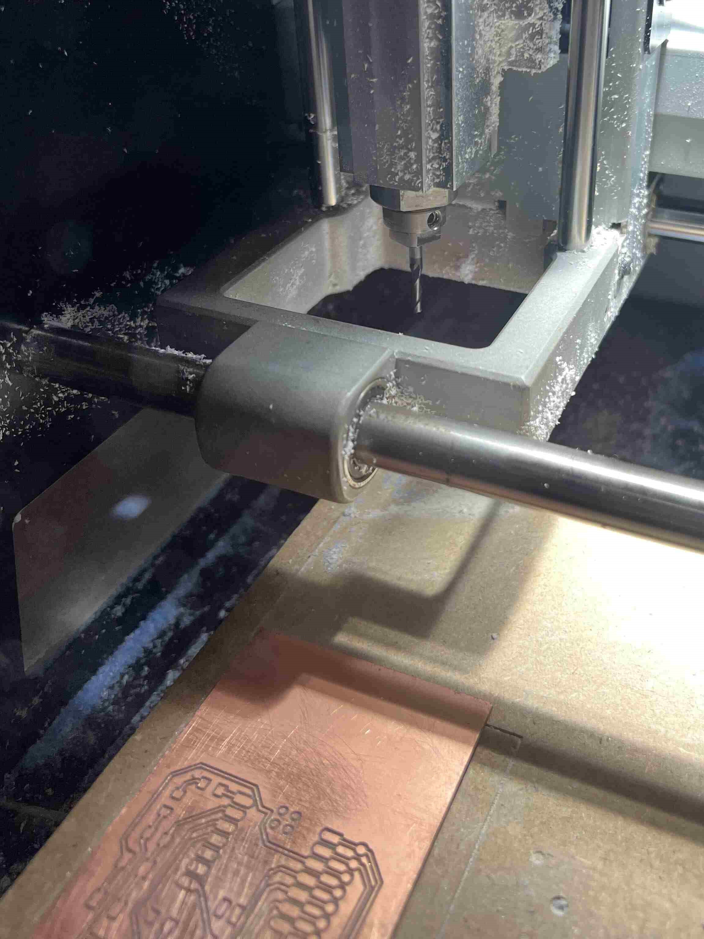
Cutting the outline
Obstacle
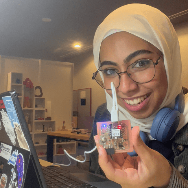
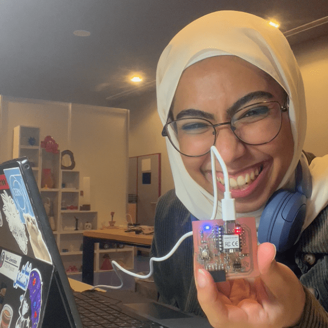
Soldering Like a Pro
PS: I burned some headers, I had to desolder them, then solder new ones, so definitely not a pro.
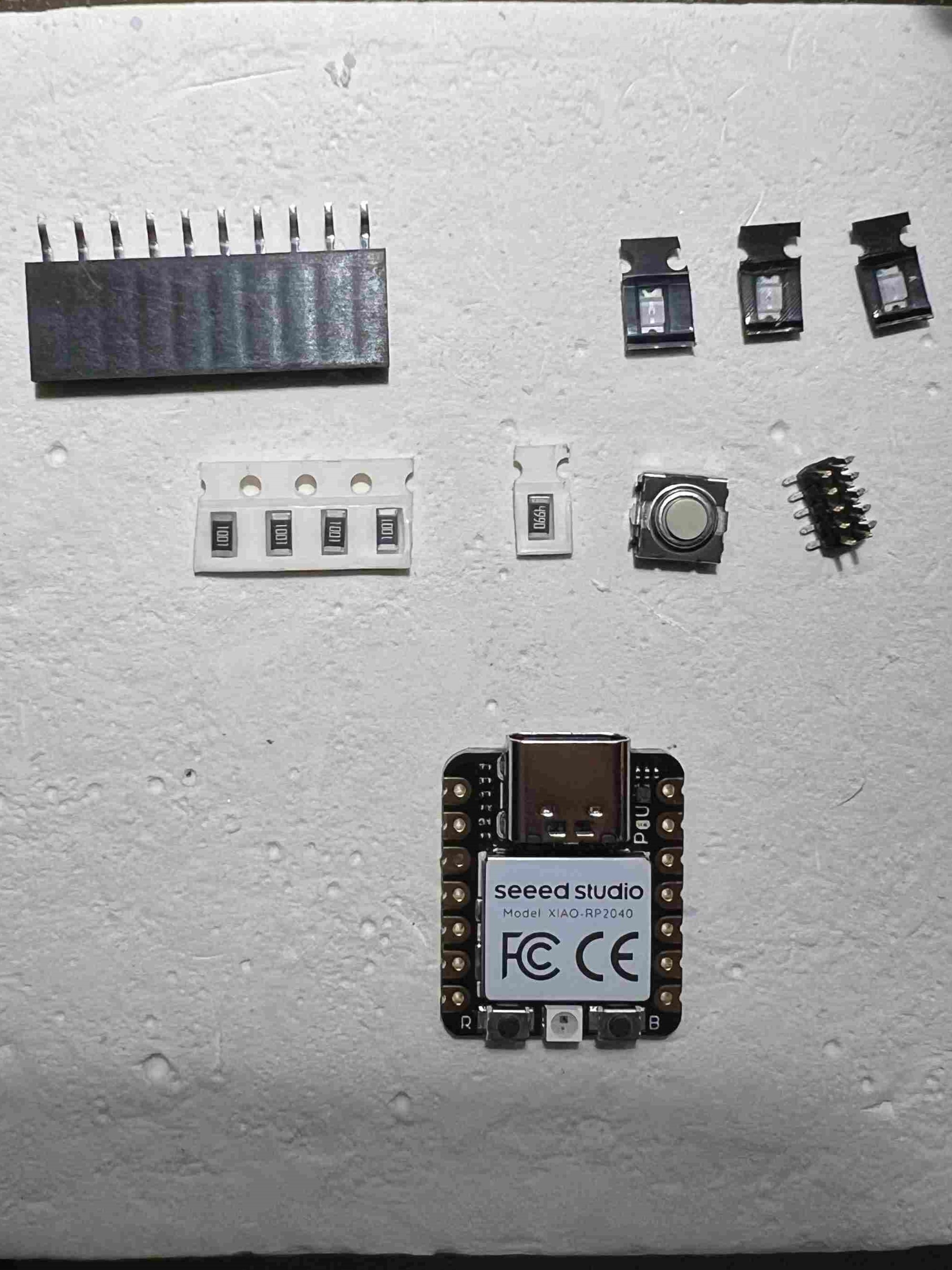
Electronics Components List:
| SEEED STUDIO XIAO RP2040 | x1 |
| RES 1K OHM 1% 1/4W 1206 | x4 |
| RES 499 OHM 1% 1/4W 1206 | x1 |
| LED CLEAR 1206 SMD | x3 |
| TACTILE SWITCH SPST | x1 |
| CONN HEADER SMD 10POS 1.27MM | x1 |
| CONN HEADER SMD R/A 6POS 2.54MM | x1 |
Checking Conductivity
Before actially powering the PCB to program it, and after soldering everything, it is good to check all things are connected the way they are supposed to be. For that, I used a multimeter, and tested the electronic components and their paths it it is connected or not. Also I had to check if they are connected to paths they are not supposed to be connected to, which will result in a short-circuit.
Does the PCB Work Now?
Spoiler Alert: It does!
Programming
After soldering, checking the conductivity in the tracks, it is time to program the PCB. For that I used Arduino IDE.